University of Warsaw
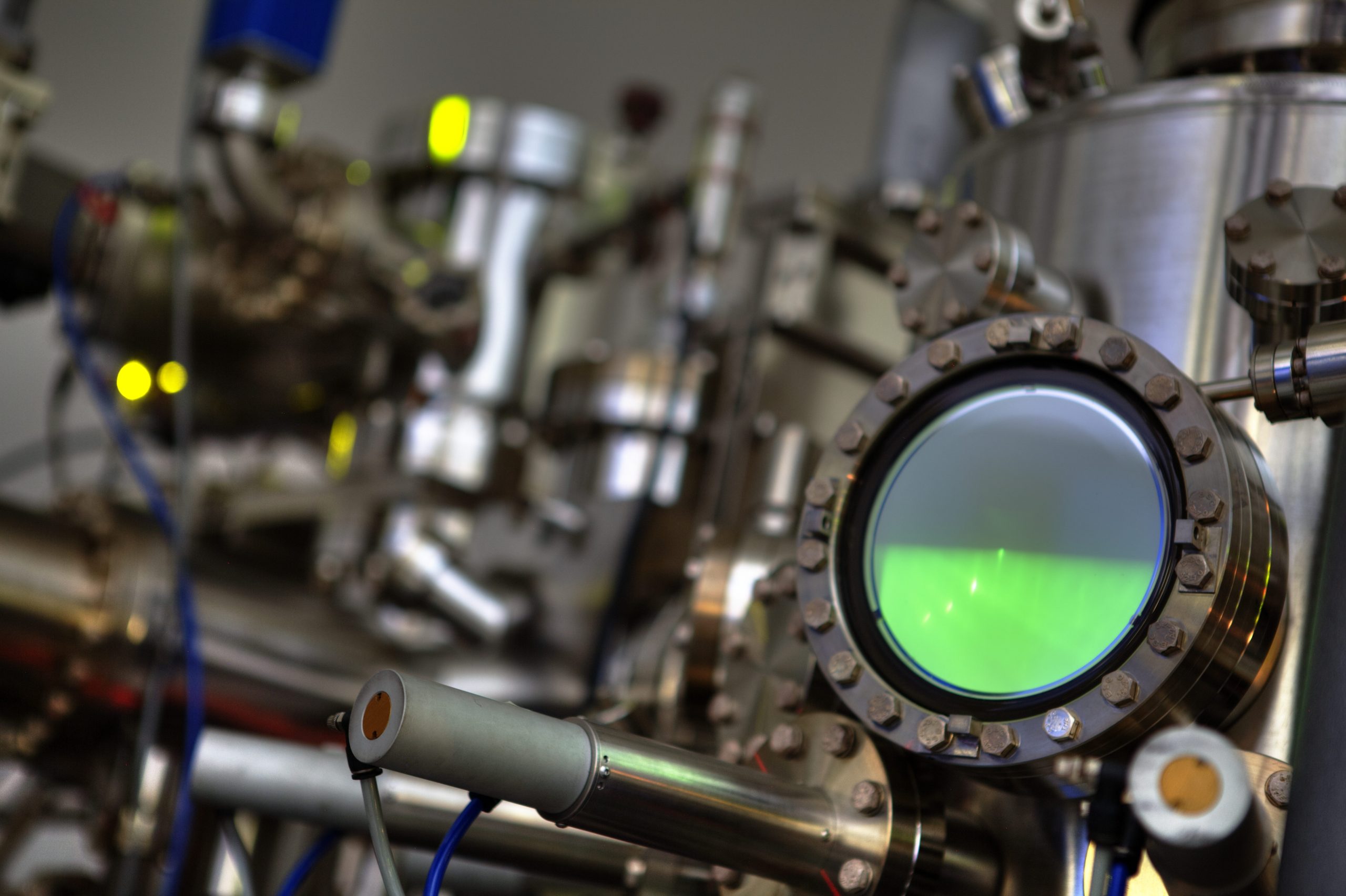
The setup enables deposition of dielectric and metallic thin films on semiconductor substrates. It uses the method of physical deposition of layers using an electron beam under vacuum conditions. Materials that can be deposited include oxides such as SiO2, TiO2 and metals such as Au, Ag, Al. It allows working with substrates with a maximum diameter of 2″. The device is equipped with an ion source, the use of which increases the homogeneity and density of the deposited layer, and quartz microbalance that allow control of the thickness of the deposited layer.
450 PLN/hour


 0000-0003-3737-464X